- 您现在的位置:买卖IC网 > Sheet目录476 > MDEV-900-HP3-SPS-USB (Linx Technologies Inc)KIT MASTER 900MHZ HP-3 USB SMD
�� �
�
�GETTING� STARTED�
�After� unpacking� the� development� system,� attach� an� antenna� to� each� board� and�
�install� the� supplied� 9V� battery.� The� development� boards� are� now� ready� for� use.�
�The� two� development� boards� are� very� similar� and� either� board� can� be� populated�
�with� a� transmitter� or� receiver� module.� The� simplex� range� testing� sections� of� the�
�boards� are� populated� differently� since,� in� the� range� testing� mode,� one� board� is�
�intended� to� serve� as� a� transmitter� and� the� other� as� a� receiver.�
�USING� THE� SIMPLEX� ENCODER/DECODER� SECTION�
�The� transmitter� board� features� a� custom� remote-control� encoder� with� two� push�
�buttons� and� the� receiver� board� features� a� decoder� with� a� relay� output� and� a�
�buzzer.� When� a� button� is� pressed� on� the� transmitter� board,� the� status� of� both�
�buttons� is� captured� and� encoded� into� a� data� stream� for� transmission.� The� data�
�recovered� by� the� receiver� is� decoded� and� the� decoder's� data� lines� are� set� to�
�replicate� the� status� of� the� encoder,� driving� either� the� buzzer� or� the� relay.�
�All� of� the� module's� connections� are� made� available� to� the� designer� via� the�
�breakout� header� (J1).� The� supplied� jumper� shunts� are� intended� to� be� placed�
�across� adjacent� pins� to� control� the� routing� of� TX� and� RX� data.�
�CHANNEL� SELECTION�
�Parallel� Selection�
�To� activate� this� area� of� the� board,� the�
�module� data� line� must� be� routed� to� the�
�encoder� /� decoder.� Configure� the�
�transmitter� board� for� encoding� and�
�transmission� by� placing� a� jumper�
�across� TX� DATA� and� ENCODER� on�
�J1�
�HOST� TX�
�TX� DATA�
�ENCODER�
�TX� MODE�
�TX� PDN�
�TX� CTS�
�J1�
�HOST� RX�
�RX� DATA�
�DECODER�
�RX� AUDIO�
�RX� MODE�
�RX� RSSI�
�All� HP3� models� feature� eight� parallel�
�selectable� channels.� Parallel� mode� is�
�selected� by� grounding� the� module's� MODE�
�line� (default� setting).� Mode� Switches� SW2�
�CS2�
�0�
�0�
�CS1�
�0�
�0�
�CS0�
�1�
�0�
�Channel�
�0�
�1�
�header� J1.� Configure� the� receiver�
�board� for� reception� and� decoding� by�
�placing� a� jumper� across� RX� DATA� and�
�DECODER� on� header� J1.�
�TX� CS2/DATA�
�TX� CS1/CLK�
�TX� CS0�
�GND�
�TX�
�RX� PDN�
�RX� CS2/DATA�
�RX� CS1/CLK�
�RX� CS0�
�RX�
�Once� the� boards� have� been�
�configured,� place� the� receiver� board� on�
�a� flat� surface� and� turn� it� on.� Turn� on� the�
�(TX) and SW3 (RX) have been provided to�
�allow� the� developer� to� easily� switch� between�
�parallel� and� serial� modes.� In� parallel� mode,�
�channel� selection� is� determined� by� the� logic�
�states� of� lines� CS0,� CS1,� and� CS2,� as� shown�
�in� the� adjacent� table.� DIP� switches� are� used�
�on� the� development� boards� to� set� the�
�0�
�0�
�1�
�1�
�1�
�1�
�1�
�1�
�0�
�0�
�1�
�1�
�1�
�0�
�1�
�0�
�1�
�0�
�2�
�3�
�4�
�5�
�6�
�7�
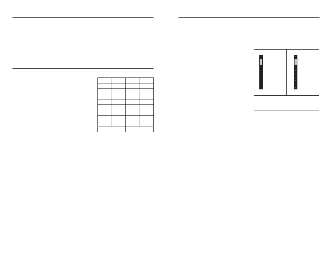
�SIMPLEX� RANGE� TEST�
�JUMPER� CONFIGURATION�
�(Factory� Default)�
�transmitter� board� and� press� button� S3.�
�You� should� hear� the� buzzer� on� the� Figure� 3:� Jumper� Configuration�
�receiver� board� sound.� You� may� now� walk� away� from� the� receiver� to� ascertain�
�the� useable� range� of� the� link� in� your� environment.�
�channels.� If� the� switch� is� set� to� ON,� then� the� 0� =� On/Low� 1� =� Off/High�
�pin� is� connected� to� ground,� otherwise� it� is�
�Table� 1:� Channel� Selection� Table�
�pulled� up� inside� the� module.� The� DIP� switch�
�positions� on� both� boards� must� match� in� order� for� the� modules� to� communicate.�
�Serial� Selection�
�In� addition� to� the� parallel� mode,� PS� versions� of� the� HP3� also� feature� 100� serially�
�selectable� channels.� The� serial� mode� is� entered� when� the� MODE� line� is� left� open�
�or� held� high.� On� the� Master� Development� boards,� this� is� accomplished� using� the�
�appropriate� Mode� Switch;� SW2� (TX)� or� SW3� (RX).� In� this� condition� CS1� and� CS2�
�become� a� synchronous� serial� port� with� CS1� serving� as� the� clock� line� and� CS2�
�serving� as� the� data� line.� The� module� is� then� easily� programmed� by� sending� and�
�latching� the� binary� number� (0-100)� of� the� desired� channel.� The� programming�
�data� is� supplied� externally� by� the� development� system� user.� Often� it� will� originate�
�from� a� microcontroller� or� emulator,� which� can� be� located� in� the� prototyping� area.�
�Using� HP3� modules� in� serial� mode� is� straightforward;� however,� minimum� timings�
�and� bit� order� must� be� followed.� Please� see� the� HP3� Series� Data� Guides� for�
�these� timings.�
�*IMPORTANT*� The� channel� selection� DIP� switch� must� be� in� the� OFF� position� in�
�order� for� the� serial� lines� to� be� used,� otherwise� the� signal� from� the� microcontroller�
�will� be� shunted� to� ground.� It� is� recommended� that� resistors� be� placed� in� series�
�on� the� data� and� clock� lines� to� limit� current� and� protect� your� microcontroller� in�
�case� the� switches� are� accidentally� turned� on.�
�Page� 4�
�Another� simple� but� often� overlooked� range-testing� method� is� to� hold� down� or�
�bridge� the� buzzer� button� so� that� a� continuous� transmission� is� made� and� then�
�walk� with� the� receiver� side� for� testing.�
�Button� S2� activates� the� relay� on� the� receiver� board.� The� relay’s� SPST� contacts�
�can� be� connected� at� J2.� Any� device� up� to� 5A� at� 30VDC� /� 120VAC� may� be�
�switched� through� the� relay.� Most� commonly,� an� external� siren� or� light� would� be�
�connected� to� aid� range� testing� if� the� on-board� buzzer� is� not� loud� enough.�
�As� you� near� the� maximum� range� of� the� link� in� your� area,� it� is� not� uncommon� for�
�the� signal� to� cut� in� and� out� as� you� move.� This� is� normal� and� can� result� from� other�
�interfering� sources� or� fluctuating� signal� levels� due� to� multipath� effects.� This�
�results� in� cancellation� of� the� transmitted� signal� as� direct� and� reflected� signals�
�arrive� at� the� receiver� at� differient� times� and� phases.� The� areas� in� which� this�
�occurs� are� commonly� called� “nulls”� and� simply� walking� a� little� farther� will� often�
�restore� the� signal.�
�To� achieve� maximum� range,� keep� objects� such� as� your� hand� away� from� the�
�antenna� and� ensure� that� the� antenna� on� the� transmitter� has� a� clear� and�
�unobstructed� line-of-sight� path� to� the� receiver� board.� Range� performance� is�
�determined� by� many� interdependent� factors.� If� the� range� you� are� able� to� achieve�
�is� significantly� less� than� specified� by� Linx� for� the� products� you� are� testing,� then�
�there� is� likely� a� problem� with� either� the� board� or� the� ambient� RF� environment� in�
�which� the� board� is� operating.� First,� check� the� battery,� switch� positions,� and�
�antenna� connection.� Next,� measure� the� receiver’s� RSSI� voltage� with� the�
�transmitter� turned� off� to� determine� if� ambient� interference� is� present.� If� this� fails�
�to� resolve� the� issue,� please� contact� Linx� technical� support.�
�Page� 5�
�发布紧急采购,3分钟左右您将得到回复。
相关PDF资料
MDEV-900-NT
TRM 900 NT MASTER DEV SYSTEM
MDEV-GPS-SG
KIT MASTER DEV GPS SG SERIES
MDEV-GPS-SR
KIT MASTER DEV GPS SR SERIES
MDEV-LICAL-HS-ES
KIT MASTER DEV HS ES RF MODULES
MDEV-USB-QS
KIT DEV MASTER USB QS SERIES
MF11-0010005
THERMISTOR NTC 100OHM -+5% PROBE
MF51E103F3950C
THERMISTOR NTC PREC -+1% 3950K
MG-300-A-9V-R
SENSOR DIGITAL GAUGE 300PSI LCD
相关代理商/技术参数
MDEV-900-NT
功能描述:射频开发工具 NT Series Dev kit w/ Transparent module
RoHS:否 制造商:Taiyo Yuden 产品:Wireless Modules 类型:Wireless Audio 工具用于评估:WYSAAVDX7 频率: 工作电源电压:3.4 V to 5.5 V
MDEV-900-TT
制造商:Linx Technologies Inc 功能描述:TRM 900 TT MASTER DEV SYSTEM 制造商:Linx Technologies Inc 功能描述:RF Development Tools TT Series Master Development System
MDEV-916-ES
功能描述:KIT MASTER DEVELOP 916MHZ ES SRS RoHS:否 类别:RF/IF 和 RFID >> 过时/停产零件编号 系列:ES 标准包装:1 系列:- 类型:用于 200/300 系列的欧盟开发套件 适用于相关产品:Zensys RF 模块 所含物品:开发板,模块,编程器,软件,线缆,电源 其它名称:703-1019Q3225667
MDEV-916-ES-RS232
功能描述:射频开发工具 ES Master Dev Sys 916MHz, RS232 Module
RoHS:否 制造商:Taiyo Yuden 产品:Wireless Modules 类型:Wireless Audio 工具用于评估:WYSAAVDX7 频率: 工作电源电压:3.4 V to 5.5 V
MDEV-916-ES-USB
功能描述:射频开发工具 ES Master Dev Sys 916MHz, USB Module
RoHS:否 制造商:Taiyo Yuden 产品:Wireless Modules 类型:Wireless Audio 工具用于评估:WYSAAVDX7 频率: 工作电源电压:3.4 V to 5.5 V
MDEV-916-SC-P
功能描述:KIT MASTER DEVELOP 916MHZ SC SRS RoHS:否 类别:RF/IF 和 RFID >> RF 评估和开发套件,板 系列:- 标准包装:1 系列:- 类型:GPS 接收器 频率:1575MHz 适用于相关产品:- 已供物品:模块 其它名称:SER3796
MDEV-916-SC-S
功能描述:KIT MASTER DEVELP 916MHZ SCS SMD RoHS:否 类别:RF/IF 和 RFID >> RF 评估和开发套件,板 系列:- 标准包装:1 系列:- 类型:GPS 接收器 频率:1575MHz 适用于相关产品:- 已供物品:模块 其它名称:SER3796
MDEV-GNSS-GM
制造商:Linx Technologies Inc 功能描述:KIT MASTER DEV GNSS GM SERIES 制造商:Linx Technologies Inc 功能描述:Master Development System for the GM Series GNSS Receiver Module 制造商:LINX TECHNOLOGIES 功能描述:Master Development System for the GM Series GNSS Receiver Module